Welcome to the home page of the Paul Braun Research Group at the University of Illinois Urbana-Champaign. Our group members perform research in the fields of materials chemistry, polymers, biomaterials, organic and inorganic self-assembly, electronic materials and photonics.
In the News
Carlos Juarez-Yescas named C2 Outstanding Mentor
Congratulations to Carlos Juarez-Yescas on being awarded the C2 (Chemical Science through Community) Outstanding Mentors for the 2023-2024 academic year. The goal of the C² program is to foster excellence in chemical sciences at Illinois.
________________________________________________________________________________________________________________
Imani Jones & Daniel Cudzich Receive Honorable Mention NSF GRFP
Braun Lab Members Imani Jones (Ph.D. Candidate) and Daniel Cudzich (Undergraduate Researcher) were recently recognized with Honorable Mention for the National Science Foundation Graduate Research Fellowship Program. Congratulations on this national academic achievement!
________________________________________________________________________________________________________________
Professor Paul Braun recipient of the 2023-2024 College Award for Excellence in Translational Research
The Grainger College Award for Excellence in Translational Research honors faculty or staff researchers for special achievement in translational research. Examples of translational research include but are not limited to: entrepreneurial activities related to research outcomes, technology transfer of research through licensing of intellectual property, and research leading directly to products/outcomes with notable societal impact.
________________________________________________________________________________________________________________
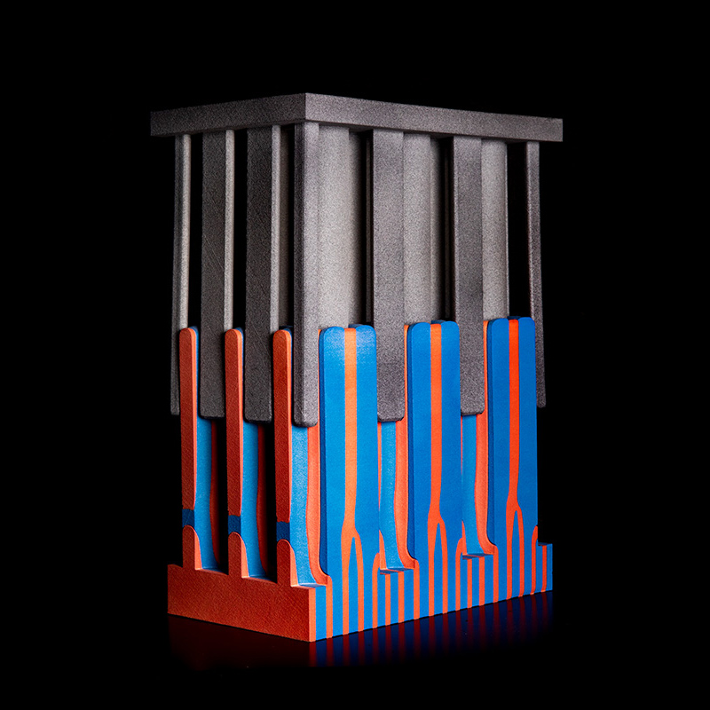
Thermally engineering templates for highly ordered self-assembled materials
Self-assembled solidifying eutectic materials directed by a template with miniature features demonstrate unique microstructures and patterns as a result of diffusion and thermal gradients caused by the template. Despite the template trying to force the material to solidify into a regular pattern, when the template carries a lot of heat it also can interfere with the solidification process and cause disorder in the long-range pattern. Researchers at the University of Illinois Urbana-Champaign and the University of Michigan Ann Arbor have developed a template material that carries almost no heat and therefore stops heat transfer between the template material itself and the solidifying eutectic material. This was accomplished by forming the template from a material with very low thermal conductivity, ultimately resulting in highly organized self-assembled microstructures.
“The key novelty of this research is that we carefully controlled the flow of heat. By controlling the flow of heat, the pattern becomes far better and more regular than before because we’re controlling more of the parameters. Previously, the template controlled the flow of atoms, but the heat flows were uncontrolled,” says Paul Braun, a professor of materials science and engineering and director of the Materials Research Laboratory, who led this research along with postdoctoral researcher Sung Bum Kang.
The results of this research were recently published in the journal Advanced Materials.
Read the full story by Amber Rose: https://mrl.illinois.edu/news/64349
Research Article: https://doi.org/10.1002/adma.202308720
________________________________________________________________________________________________________________
Read More Braun Lab News
| Braun Group Recent Publications |
|---|
| X. Yan, J. Diamond, N. Fritz, S. Matsuo, K.F. Rabbi, I. Zarin, N. Miljkovic, P.V. Braun and N. Sottos, Nickel-Silicon Interfacial Adhesion Strength Measured by Laser Spallation, Journal of Applied Physics, 135, 16, 165302 (2024). DOI: 10.1063/5.0198331 |
| S.B. Kang, G. Huang, G. Singhal, D. Xie, D. Hsieh, Y. Lee, A.A. Kulkarni, J.W. Smith, Q. Chen, K. Thornton, S. Sinha and P. V. Braun, Highly Ordered Eutectic Mesostructures via Template-Directed Solidification within Thermally Engineered Templates, Advanced Materials, 36, 15, 2308720 (2024). DOI: 10.1002/adma.202308720 |
| Y.B. Lee, B.A. Suslick, D. de Jong, G.O. Wilson, J.S. Moore, N.R. Sottos, P.V. Braun, A Self-Healing System for Polydicyclopentadiene Thermosets, Advanced Materials, 36, 11, 2309662 (2024). DOI: 10.1002/adma.202309662 |
| Y. Kim, C. Juarez-Yescas, D.W. Liao, M.K. Jangid, P. Joshi, H. Yang, B. Zahiri, P. Braun and N. Dasgupta, Thin Free-Standing Sulfide/Halide Bilayer Electrolytes for Solid-State Batteries Using Slurry Processing and Lamination, ACS Energy Letters, 9, 4, 1353-1360 (2024). DOI: 10.1021/acsenergylett.4c00092 |
| Z. Cheng, Yu-Ju Huang, B. Zahiri, P. Kwon, P.V. Braun and D.G. Cahill, Ionic Peltier Effect in Li-Ion Electrolytes, 26, 6708-6716 (2024). DOI: 10.1039/D3CP05998G |
| Y-Y, Lin, C. Juarez-Yescas, K-W. Lan, P.V. Braun, J.A. Krogstad, and N.H. Perry, Isolation of Grain vs. Intergranular Transport in Li1+xTixTa1-x SiO5 Suggests Concerted Ion Migration in a High-Voltage Stable Electrolyte from High-Throughput Descriptors, ACS Applied Energy Materials, 6, 22, 11468-11480 (2023). DOI: 10.1021/acsaem.3c01647 |